
AI 101 — What is HBM (high-bandwidth memory)?

HBM is the stacked memory package that an AI accelerator's processor can read from and write to many times faster than normal RAM — and right now it is the single most expensive, scarcest part of the AI buildout. If you have read that the memory shortage is raising chip prices, throttling roadmaps, or forcing startups to rethink fabs, HBM is the "memory" in that sentence. This is the ten-minute version.
It matters today for one plain reason: every frontier AI chip depends on it, and there is not enough of it. AI demand sold out all 2027 DRAM and HBM capacity, Chinese accelerator prices jumped 20% to 50% in two months because of it, and a single HBM4 stack now sells for around $392. Nvidia is reportedly testing versions of its next Rubin Ultra accelerator with as little as 192 GB of memory — down from the 1 TB it announced — because HBM4E supply cannot keep pace. That is not a supply-chain footnote; it is design decisions being made at the flagship level.
The one-paragraph mental model
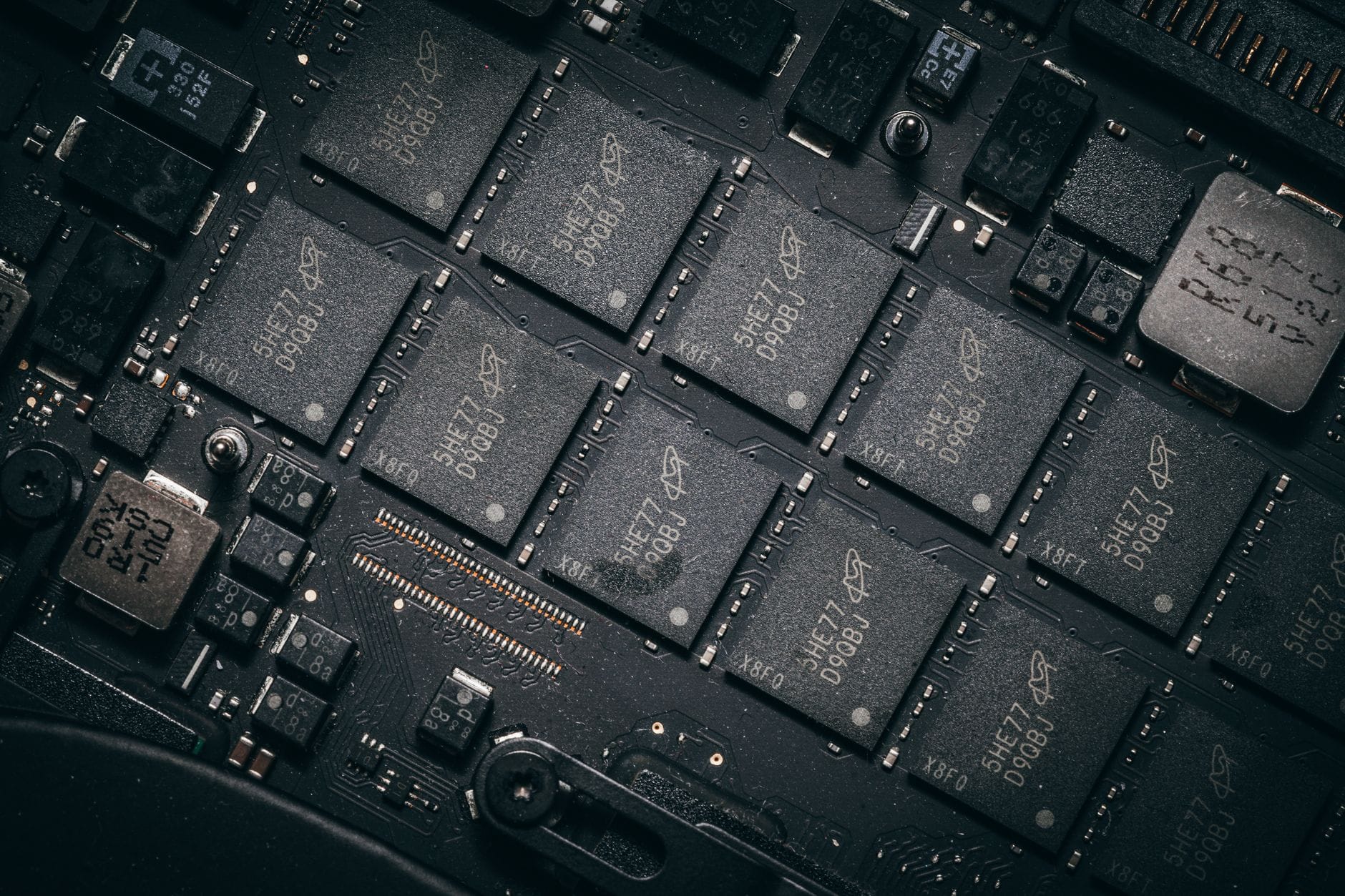
Memory has two separate jobs: holding a lot of data, and delivering it fast. Ordinary DDR memory in your laptop is excellent at the first and mediocre at the second. HBM gets both by changing the shape of the chip instead of just speeding up the clock. It takes several flat DRAM dies, drills vertical connections called through-silicon vias through each one, stacks them like a tower of very thin pancakes, and sits that tower on a silicon interposer right next to the processor die. Because the memory is physically adjacent and connected by thousands of tiny wires rather than a few dozen long ones, the data path is extremely wide: a single HBM stack talks over a 1024-bit interface, against 32 bits for a conventional GDDR memory chip. A wide road carrying traffic at a modest speed moves more per second than a narrow road at twice the limit — that is the whole trick. The cost is manufacturing: Micron notes that an HBM3E die can push about 256 GB/s against roughly 8 GB/s for a DDR5 die, but reaching it takes 256 banks running in parallel and extra die area for data paths, power delivery and those vias.
The analogy: a supermarket with a thousand checkout lanes
Picture a warehouse full of everything a kitchen needs. The processor is a chef who can chop at absurd speed. Ordinary memory is a warehouse with four loading docks: plenty of storage, but if the chef needs a truckload of ingredients every minute, everything queues at the dock. HBM does not make the warehouse bigger or the trucks faster — it builds a thousand loading docks along one wall and puts the warehouse right next door. Same ingredients, same trucks, but the queue disappears. What HBM cannot do is change the fact that a chef who finishes chopping and waits for ingredients is a chef standing still. That wait has a name in the industry — the memory wall — and it is why HBM is now the most contested silicon on earth.
What people get wrong
"HBM is just fast RAM you could swap in anywhere." It is not a drop-in part. The interposer and the thousands of connections between stack and processor mean HBM has to be designed into the package from the start, and TSV tooling is the main bottleneck when memory makers try to convert ordinary DRAM capacity into HBM capacity.
"More HBM means a smarter model." It means a model that is not waiting around. Bandwidth determines how fast tokens come out; it does not raise quality. A model's reasoning is unchanged by the memory underneath it.
"HBM is only about capacity." Capacity and bandwidth are separate axes. You can have a large stack that still starves the chip, and a smaller one that feeds it well. The current shortage is forcing both down together, which is why accelerator roadmaps are being cut.
"The next generation fixes the shortage." HBM4 doubles the interface to 2048 bits and reaches up to about 2 TB/s per stack under the JEDEC specification released in April 2025, but it does not make fabs appear. Samsung is now building its HBM4 base dies on a 4-nanometer logic process, and Nvidia's custom NVHBM moves the memory controller into the stack itself — both are engineering answers to cost and power, not supply answers.
Where to learn more
Start with the JEDEC standards body that defines each generation, then read Micron's and SK Hynix's product pages for the current shipping stack heights and speeds. SemiAnalysis's HBM roadmap piece is the deeper industry read if you want the manufacturing detail. Two of our own explainers pair well with this one: What is a context window? explains the other way memory constrains a model, and What is model quantization? covers the main trick for fitting a big model into less of it.
If HBM supply — not model quality — is what decides how fast AI advances, is that a temporary crunch or the new normal? Tell us in the comments.
Sources: Wikipedia — High Bandwidth Memory · SemiAnalysis — Scaling the Memory Wall: The Rise and Roadmap of HBM · NVIDIA DGX B200 specifications · AI Midday — AI demand sold out all 2027 DRAM and HBM capacity · AI Midday — Samsung moves HBM base dies to a 4nm logic node